 |
| The NAND Gate (Schematic symbol and truth table) |
The 74xx00 contains 4 NAND gates which each independently consist of 2 inputs, A, B, and one output C (Pin names are arbitrary; they could also be inputs, P, Z and output, X) The NAND gate is considered universal because a configuration of NAND gates can function as all the logic gates: AND, OR, NOT, NOR, NAND, XOR, XNOR. For example, to form a NOT gate purely of NAND gates would one input to be in contact with the other, so that only one value (1 or 0) enters both of the inputs. Doing that cuts out the two middle sections of the truth table shown above. Creating other logic gates by means of NAND gates is called NAND Implementation. So, with one 74x00 integrated circuit chip you could create two NOT gates. That is less efficient than just using a 74x04 chip, but may be preferred when purchasing chips in bulk. Prices are low in bulk purchases, and only having one type of gate can save employees or engineers the trouble of reading which chip they are using because they all would be 74x00.
Here is a MultiSim snapshot of all other types of gates using only NAND gates. This is known as NAND logic implementation.
 |
| MultiSim 8 screenshot of NAND Implementation |
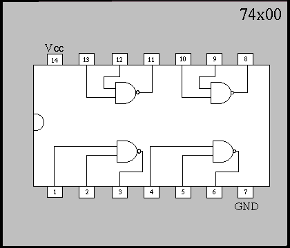 |
| 74x00 Pin out diagram. Vcc is power and GND is ground. |


No comments:
Post a Comment