w7r.blogspot.com

Introduction to the Clocked SR latch
The clocked SR latch (sometimes "Gated SR Latch") is a modification to the Set-Reset Latch (SR latch). After adding the clock to the design, the SR latch can control when it should switch states (when Q and Q' switch values).
Enable To The Rescue
The inputs S and R are meaningless unless the enable input is true. The enable input is the clock input so the circuit is considered "enabled" when CLK=1 on a positive triggered SR latch and when CLK=0 on a negative triggered SR latch.
What's a Clock?
A clock is an element that produces both 1 and 0's, and does so in both regular intervals (like a timer) and irregular intervals (button on arcade game).

The Clocked SR-Latch Design
The clocked SR latch is established by adding 2 AND gates (positive triggered) or 2 NAND gates to filter out the data on the S and R nodes when undesired. This design provides a short term fix to a big problem, the unpredictable state at S=1 and R=1 (given the clock is being triggered CLK=1). to the SR-latch design of 2 NAND or 2 NOR gates. Take a look at the pictures for a more thorough understanding of the design.
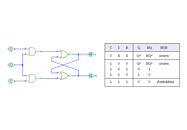 |
| This clock is positive edge triggered. For the design to be negative edge triggered the AND gates would be NAND gates. |
| Clocked Set-Reset Latch Table (+ edge) | |||||
|---|---|---|---|---|---|
| CLK | S | R | Q | Q' | Description |
| 0 | X | X | Q | Q' | No change in Q and Q' |
| 1 | 0 | 0 | Q | Q' | No change in Q and Q' |
| 1 | 0 | 1 | 0 | 1 | Clear Q |
| 1 | 1 | 0 | 1 | 0 | Set Q |
| 1 | 1 | 1 | ? | ? | Undesirable state |


